LPDDR5
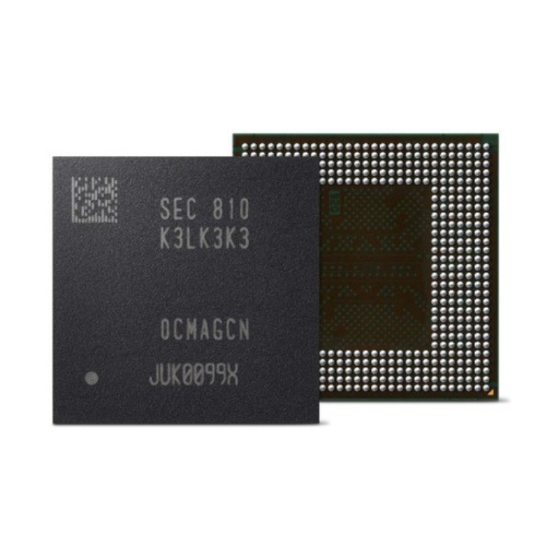
Basic Identity Recognition 1. Manufacturer Identification: SEC = Samsung Electronics (Samsung Electronics), 810 represents the production batch/year code 2. Core Model: K3LK3K3, the complete part number is K3LK3K30EM-BGCN (the latter part of OCMAGCN in the figure corresponds to the suffix BGCN) 3. Product Type: The world's first 10nm-class LPDDR5 mobile DRAM memory chip, released by Samsung in 2018 4. Packaging Form: 496-ball F-BGA flip-chip ball grid array packaging, with a dense array of solder balls visible on the back in the figure
LPDDR5
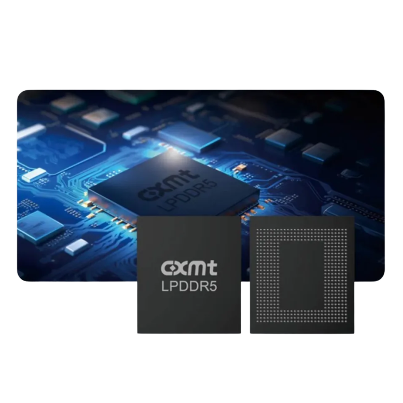
ChangXin Storage CXMT LPDDR5 Domestic Mobile Memory I. Basic Identity Identification 1. Manufacturer Identification: CXMT = ChangXin Memory Technologies Co., Ltd., the first indigenous manufacturer in Mainland China to mass-produce DRAM. 2. Product Type: LPDDR5 mobile DRAM memory chip, the first domestically developed and independently researched LPDDR5 specification die in China. 3. Packaging Form: FBGA Ball Grid Array packaging (the solder ball matrix on the back is visible on the right side of the figure), compatible with packaging standards of international manufacturers such as Samsung and SK Hynix.
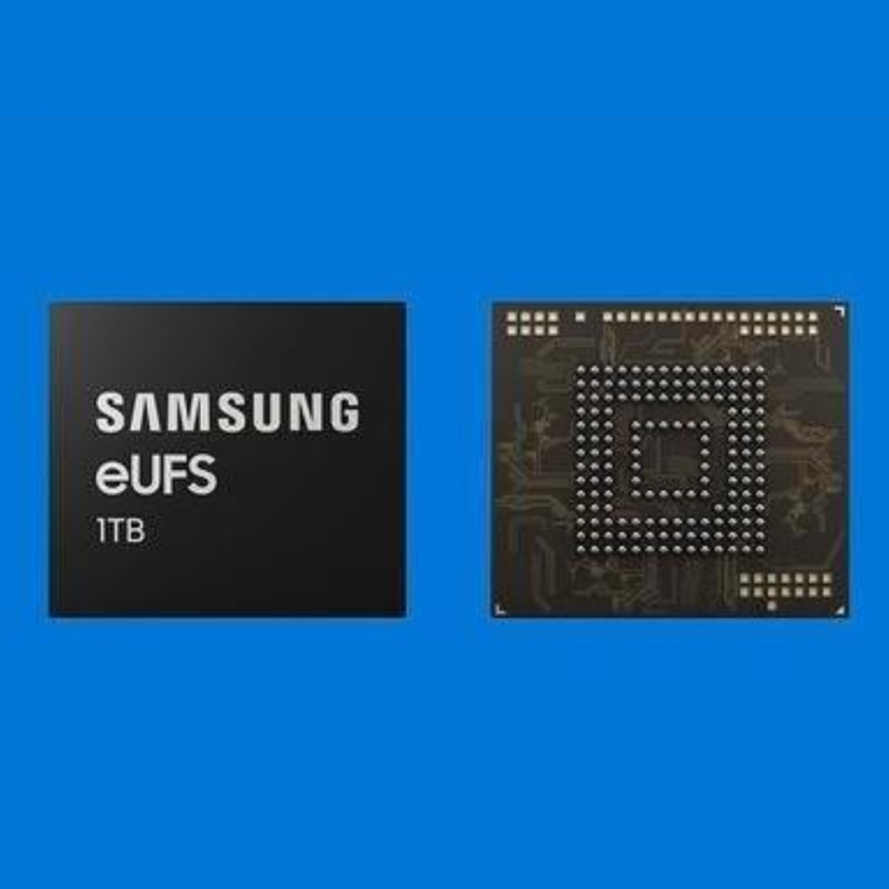
1TB eUFSE mbedded Flash memory
Brand: SAMSUNG Electronics (a leading global flash memory manufacturer). 2. Product Type: eUFS (embedded Universal Flash Storage), an embedded universal flash storage used as the internal storage (hard drive) for smartphones and tablets, which is completely distinct from the previous LPDDR RAM. 3. Capacity Specification: 1TB in a single package. 4. Package Form: 153-ball FBGA (Flip-Chip Ball Grid Array) package. The image on the right shows the solder ball array on the chip's backside. It has a standard size of 11.5×13.0mm and is compatible with mobile device motherboards.