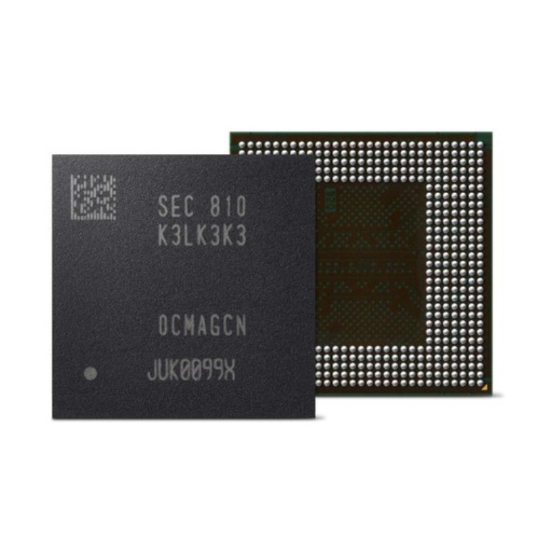
LPDDR5
rformance comparison with the previous generation (LPDDR4X) • Approximately 50% higher bandwidth and approximately 20% lower power consumption • Supports high-load scenarios such as 5G baseband, AI computing, high-refresh-rate mobile screens, and multi-camera image processing • Introduces new power management and adaptive refresh mechanisms for significantly improved battery life
Technical Highlights 1. Adopting a multi-bank architecture to reduce multi-task access latency. 2. Independent low-power I/O voltage domain, resulting in significantly reduced standby power consumption. 3. Compatible with JEDEC LPDDR5 standard, enabling smooth upgrade to LPDDR5X specification in the future. 4. BGA large ball grid array packaging, offering superior heat dissipation and signal integrity compared to previous generation LPDDR4 dies.
Core Hardware Parameters Table
Parameter Item Specification Value
Storage Density 64Gb (8GB per die capacity)
Data Rate 5500 Mbps (Equivalent Bandwidth 51.2GB/s)
Bit Width Architecture x64-bit
Operating Voltage Multi-level low voltage: 1.8V/1.05V/0.9V/0.5V
Operating Temperature -25℃ ~ 85℃ (Consumer Mobile Device Standard)
Process Technology 10nm-class EUV Process